-
Notifications
You must be signed in to change notification settings - Fork 86
mi0bot edited this page Nov 9, 2020
·
15 revisions
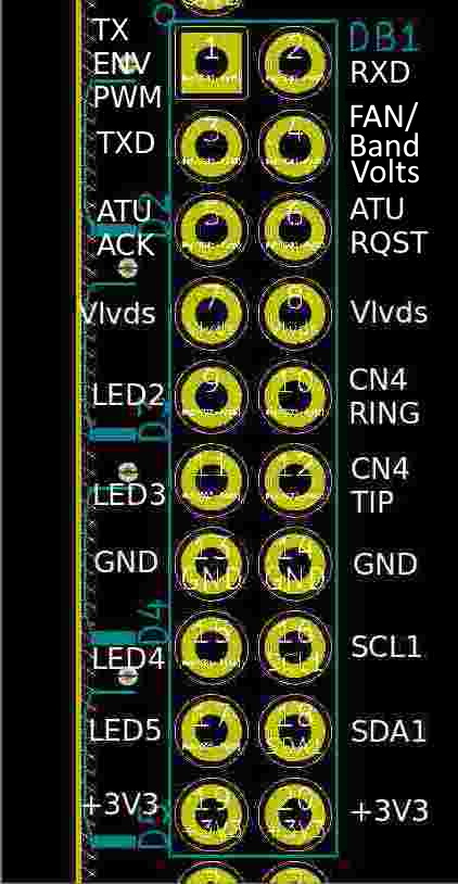
This is the tentative IO assignment for the standard HL2 gateware. It is still possible to have options in the main gateware that when enabled use the IO differently for pins marked GW.
DB1, near LEDs. Schematic page 6, A2:
| Pin | IO | Assignment | GW |
|---|---|---|---|
| 1 | 2.5V IO | TX Envelope PWM | GW |
| 2 | 2.5V IO | RXD UART | GW |
| 3 | 2.5V IO | TXD UART | GW |
| 4 | 2.5V IO | FAN or BAND VOLTS PWM | GW |
| 5 | 2.5V IO | ATU ACK | GW |
| 6 | 2.5V IO | ATU RQST | GW |
| 7 | - | VLDS | |
| 8 | - | VLDS | |
| 9 | - | D2 LED | |
| 10 | - | CW/PTT Ring | |
| 11 | - | D3 LED | |
| 12 | - | CW/PTT Tip | |
| 13 | - | GND | |
| 14 | - | GND | |
| 15 | - | D4 LED low | |
| 16 | - | SCL1 | |
| 17 | - | D5 LED low | |
| 18 | - | SDA1 | |
| 19 | - | 3v3 | |
| 20 | - | 3v3 |
| Pin | IO | Assignment | GW |
|---|---|---|---|
| DB12-1 | 2.5V LVDS IO | TXN | |
| DB12-2 | 2.5V LVDS IO | TXP | |
| DB12-5 | 2.5V LVDS I | RXN | |
| DB12-5 | 2.5V LVDS I | RXP | |
| CN8-1 | 3.3V I | TX Inhibit | GW |
| CN9-1 | 3.3V I | GW | |
| CN10-1 | 3.3V I | Temporary MAC Alternate | GW |
| TP2 | 2.5V I | GW | |
| TP7 | 3.3V I | GW | |
| TP8 | 3.3V I | GW | |
| TP9 | 3.3V I | GW |
- 40mm End Plate with notes for 40mm and 55mm
- 55mm End Plate use notes from above
- DB-9 Level Shifter Board
- PureSignal Feedback
- Small IO Expansion
- Alternate HL2/N2ADR Jumper with PureSignal Feedback and IO Expansions
- Alex Pressl's HL2 Breadboard
Notes from LB1HI on use of and experimentation with various IO boards.

