A development board for the STM32MP1 Application Microprocessor with all MPU pins routed through to 2.54mm headers. No exotic proprietary connectors needed!
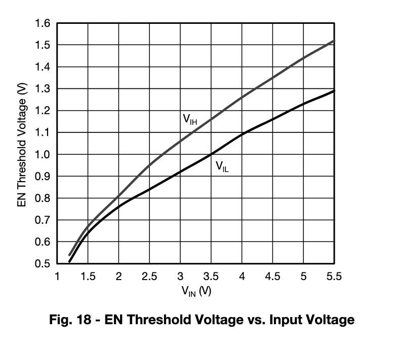
The power supply requirements for microprocessors are always complicated. I decided to use a discrete power supply scheme using a single LDO for the main 3.3V rail, a buck regulator for the DDR 1.35V rail and a load switch to detect the USB 1.8V rail. The latter comes from an internal regulator ands powers the VDD3V3_USBFS and VDD3V3_USBHS. This needs to be enabled only after the 1.8V rail comes up, so this needs to be enabled using a MOSFET. However, you need to pick a transistor that will fully switch on for 1.8V Vgs. After having some issues I played it safe with a load switch: the SIP3250, which turns on as low as 1.2V...according to the datasheet
The characteristics seem to back this up until you get to the Fig.10. Perhaps not quite as good as 1.2Vgs but even at 1.5Vgs, this is more than good enough for these requirements.
 |
 |
|---|
Whether this is too much hassle when you can use a single PMIC is debatable. The sheer number of passive components needed to support a PMIC is eye-watering.
The table below lists the power supply scheme on this board:
| Power Supply Rail | MPU Pin Name | MPU Pin # | Comment |
|---|---|---|---|
| 3.3v | VDD VBAT VDD_PLL VDD_PLL2 VDD_ANA VDD_DSI PDR_ON_CORE PDR_ON |
K6 H3 J5 G13 L3 A12 N1 N2 |
Linear regulator (SE8233X2) |
| 3.3v | VDDA VREF+ |
M4 N3 |
via inductor L3 If JP4 is connected (default) |
| 3.3v | VDD3V3_USBFS VDD3V3_USBHS |
W12 W15 |
via NMOS (DMG2302U) when 1.85v rail is detected from MPU |
| 1.35v | VDD VDDQ VDDCORE VDDQ_DDR |
B2 A1 E7 E15 |
Buck regulator TPS54202 |
| 1.85v | VDDA1V8_REG | V11 | Internal regulator, externally connect to VDDA1V8_DSI (B12) |
| 1.2v | VDD1V2_DSI_REG | B16 | Internal regulator, externally connected to VDD1V2_DSI_PHY (A16) |
| 1.1v | VDDA1V1_REG | W11 | Interal regulator, internally connected. |
Note: 3.3v rail is also connected to:
- SWD debug interface
- SDIO connectors (microSD)
- pull-ups for the BOOT pins
- external power output on the pin headers (pin #26 on J1, J2, J3, J4)
| Overview | Power Supply |
|---|---|
| STM32MP1 Power | STM32MP1 DDR |
|---|---|
| STM32MP1 GPIO | STM32MP1 Debug |
|---|---|
Before we boot the board with a Linux image. It is helpful to check the MPU is alive and responding. We can use the SEGGER JLink to connect to the cores via the SWD connector (J6).
BOOT pins must be set to B0 and B2.
JLinkExe -device STM32MP15XX_A7_0_DUALFLASH -if SWD -speed 4000 -autoconnect 1
SEGGER J-Link Commander V6.98a (Compiled Mar  5 2021 17:04:44)
DLL version V6.98a, compiled Mar  5 2021 17:04:29

Connecting to J-Link via USB...O.K.
Firmware: J-Link V11 compiled Feb  4 2021 12:59:17
Hardware version: V11.00
S/N: 261002652
License(s): FlashBP, GDB
OEM: SEGGER-EDU
VTref=3.341V
Device "STM32MP15XX_A7_0_DUALFLASH" selected.


Connecting to target via SWD
ConfigTargetSettings() start
ConfigTargetSettings() end
InitTarget() start
InitTarget() end
Found SW-DP with ID 0x6BA02477
DPIDR: 0x6BA02477
AP map detection skipped. Manually configured AP map found.
AP[0]: AXI-AP (IDR: Not set)
AP[1]: APB-AP (IDR: Not set)
AP[2]: AHB-AP (IDR: Not set)
Using preconfigured AP[1] as APB-AP
AP[1]: APB-AP found
Found Cortex-A7 r0p5
6 code breakpoints, 4 data breakpoints
Debug architecture ARMv7.1
Data endian: little
Main ID register: 0x410FC075
I-Cache L1: 32 KB, 512 Sets, 32 Bytes/Line, 2-Way
D-Cache L1: 32 KB, 128 Sets, 64 Bytes/Line, 4-Way
Unified-Cache L2: 256 KB, 512 Sets, 64 Bytes/Line, 8-Way
System control register:
  Instruction endian: little
  Level-1 instruction cache enabled
  Level-1 data cache enabled
  MMU enabled
  Branch prediction enabled
Memory zones:
  Zone: Default Description: Default access mode
  Zone: APB-AP (AP1) Description: DMA like acc. in AP1 addr. space
  Zone: AHB-AP (AP2) Description: DMA like acc. in AP2 addr. space
Cortex-A7 identified.
BOOT pins must be set to B2 only.
JLinkExe -device STM32MP15XX_M4_DUALFLASH -if SWD -speed 4000 -autoconnect 1
SEGGER J-Link Commander V6.98a (Compiled Mar  5 2021 17:04:44)
DLL version V6.98a, compiled Mar  5 2021 17:04:29

Connecting to J-Link via USB...O.K.
Firmware: J-Link V11 compiled Feb  4 2021 12:59:17
Hardware version: V11.00
S/N: 261002652
License(s): FlashBP, GDB
OEM: SEGGER-EDU
VTref=3.342V
Device "STM32MP15XX_M4_DUALFLASH" selected.


Connecting to target via SWD
ConfigTargetSettings() start
ConfigTargetSettings() end
InitTarget() start
InitTarget() end
Found SW-DP with ID 0x6BA02477
DPIDR: 0x6BA02477
AP map detection skipped. Manually configured AP map found.
AP[0]: AXI-AP (IDR: Not set)
AP[1]: APB-AP (IDR: Not set)
AP[2]: AHB-AP (IDR: Not set)
AP[2]: Core found
AP[2]: AHB-AP ROM base: 0xE00FF000
CPUID register: 0x410FC241. Implementer code: 0x41 (ARM)
Found Cortex-M4 r0p1, Little endian.
FPUnit: 6 code (BP) slots and 2 literal slots
Detection of Coresight components via ROM table search disabled by user
Cortex-M4 identified.
Here is a photo successfully connecting to the A7 core on the assembled board using JLink (via SWD). It lives!


